


- PID
- 3294002
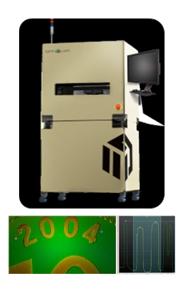
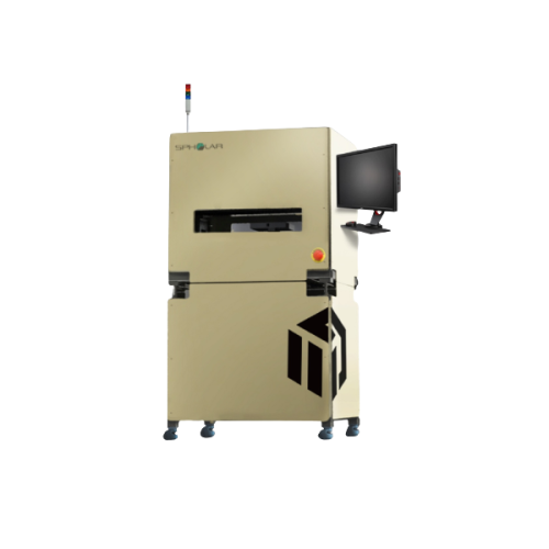
3D Surface Depth Measurement Inspection Device
- Certification
-
- Award
-
- Shipping
-
- Lead Time7 ~ 30days
- Modes of Transport CIF,FOB
- Products Shipped From Incheon
- Payment
-
140+ Global Payments, trusted and secure payment provided by PayVerse.
Learn More
- Quantity
- MOQ : 5 Units
Detailed Description
The 3D surface measurement inspection device
∙Product overview
: Used for inspection of semiconductor wafers and devices, an inspection of photomasks and reticles used in semiconductor manufacturing, transparent translucent materials or metal properties, and internal and external inspection of objects for defect detection in the product manufacturing process. Checking the process result after the process of the manufacturing line, preventing the leakage of defects, and managing the yield
∙Use-For research and development :
3D shape measurement, size measurement, surface and depth inspection
-For manufacturing production: manufacturing line defect, internal crack inspection, yield management, etc.
-Medical, shipbuilding, and future car sectors: various applications by industry group
∙Main specifications (can be made to order)
-Horizontal resolutions: sub um~ several um-Vertical resolution: sub um~ several um
-Vertical measurement range: ~ 5mm
-Measurement speed: 1 second or less (1 AREA per FOV or 100,000 points scan/1 second)
∙Main features
-Excellent product quality with excellent research personnel
-Resistant to vibration (measured without mechanical movement)-No products with the same specifications either domestic or abroad
-Price competitiveness compared to competitors