- PID
- 3120747
- Blocked seller
CCL- PCB-MOBILE PHONE-SQUARE-MULT-COLOR
Request For Quotation
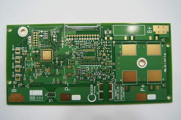
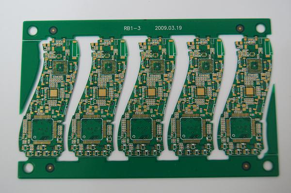
PCB(PRINTED CIRCUIT BOARD)
- Award
-
- Shipping
-
- Payment
-
140+ Global Payments, trusted and secure payment provided by PayVerse.
Learn More
Detailed Description
Copper wiring boards are thinly printed boards. They are used to connect various parts such as semiconductors, capacitors, resistors, etc., and serve to connect the parts. PCBs are designed to reduce the size and performance of electronics by allowing efficient design of electrical wiring
Rigid-flexible (R-F) PCBs that combine rigid (flexible) and rigid (rigid-flexible) PCBs.
(Nx 2) layer PCB depending on how many layers the circuit is overlapped with, and the raw material (FR-2) which is commonly used for rigid board manufacture from three or more layers (multilayer) 4) Due to the nature of PCBs in odd-numbered layers
Although the substrate itself can be used as an insulator, it may be printed on glass (automotive rear glass heating wire) or vinyl (keyboard contact point), but usually the resin (prepreg, PP) .
Here is the formal method:
1. Scrubbing copper plate or peeling off copper film through ethanol (front, Scrubbing)
2. Apply a sensitizing solution on the copper plate (Lamination, Lamination).
3. Print the substrate on transparent vinyl, cover it on the photosensitive liquid, and apply ultraviolet rays (exposure, Exposing).
At this time, only the portion of the photosensitive liquid exposed to the ultraviolet ray is cured and the coating remains.
4. Wash the sensitizing solution and immerse it in ferric chloride solution (Etching, Etching).
Keeping the solution warm and rubbing it with a sponge can be done faster. The thing to note is that if you immerse too long at this time, you can melt to where you should not melt. The ferric chloride solution should not be exposed to the skin.
5. If all copper plates are not melted, remove the PCB, rinse it, and peel off the coating with ethanol or thinner. (Strip)
Keyword
Product Data
Other products of this company
