- PID
- 3045265
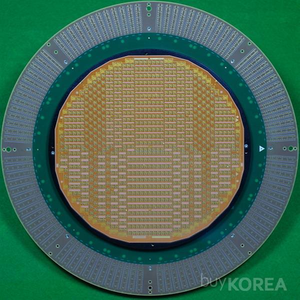
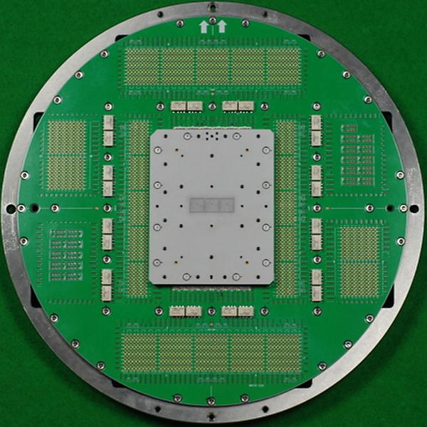
Semiconductor Wafer Test Probe Card
Request For Quotation
Semiconductor Wafer Testing, Probe Card, Nand Flash, DRAM, System on Chip, EDS, Wafer, Probing, MEMS Probe, Cantilever
- Award
-
- Shipping
-
- Payment
-
140+ Global Payments, trusted and secure payment provided by PayVerse.
Learn More
Detailed Description
[Semiconductor Wafer Test Probe Card]
* Memory Application: NAND Flash, DRAM
* Non-memory Application: SoC (Vertical), CIS (MEMS), DDI, DC Parametric etc.
A probe card is an interface between an electronic test system and a semiconductor wafer. Its purpose is to provide an electrical pathway between a test system and the circuits in a wafer, thereby permitting the testing and validation of the circuits at the wafer level, usually before they are diced and packaged.
Keyword
Product Data
Other products of this company
